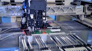
Next, a solder mask is applied to protect the copper traces and to prevent short circuits. Component placement machines then position and solder the various components onto the board, ensuring precise alignment and proper connection. Once the components are in place, a final protective layer is applied, and the pcb assembly is inspected for quality and functionality.
Quality control is a critical part of PCB fabrication, as even minor defects can lead to malfunctioning electronic devices. Inspection processes may include visual checks, electrical testing, and X-ray analysis to verify the integrity of the board and its components.
In recent years, the PCB fabrication process has seen significant advancements. These include the development of smaller and more densely packed boards, the use of surface-mount technology (SMT) for smaller and lighter components, and the adoption of more eco-friendly manufacturing processes.
As technology continues to evolve, so too does the PCB fabrication process. With the demand for smaller, more powerful electronic devices and the push for sustainable manufacturing, the PCB industry will undoubtedly continue to innovate and adapt to meet the ever-changing needs of the electronics market. PCB fabrication remains a cornerstone of the electronics industry, ensuring that our devices continue to get smarter, more efficient, and more interconnected.